
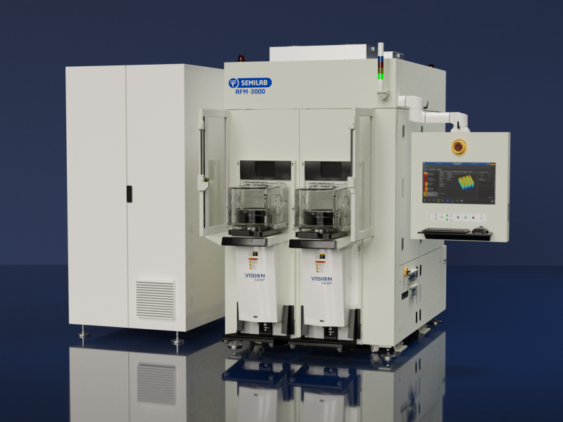

The Semilab AFM-3000 system is designed for various applications, including:
-
Particle Inspection:
- Precise defect localization through the light scattering method (μPIT).
- Defect inspection using a high-resolution AFM scanner based on imported KLARF files.
-
CMP Process Control:
- Consistent and highly reproducible roughness characterization for quality control of semiconductor wafers up to 12″ (300 mm).
-
Critical Dimension AFM:
- Provides detailed 3D sample surface information on micro and nano scales.
- Suitable for silicon and non-silicon wafers, thin films, and surfaces with nanotopography.
Key Features:
- Provides high-resolution, sub-atomic precision measurements with extremely low noise levels.
- Ensures stable and accurate performance in a customizable, user-friendly environment.
- Offers vibration isolation and supports variable cantilever types with outstanding scan rates.
- Equipped with a wafer contour meter for repeatable and precise alignment.
- Includes a full wafer AFM profilometer mode.
- Optional advanced defect review capability, combining high-resolution AFM measurement with micro-particle inspection metrology (mPIT) for immediate defect determination.
- Features pattern recognition.
- Provides a low-noise platform.
- Offers flexibility with AFM tip scanner setup for a wide scanning range.
- Accommodates sample sizes up to 300 mm.
Specifications:
- Automated system with a new platform, featuring fully automated sample loading, data evaluation, and factory integration.
- Low noise platform with high-performance acoustic and active vibration isolation.
- Precise positioning stage.
- µPIT capability for the precise localization of defects.
- Customizable Software with KLARF defect file import.
- Full wafer area accessibility.
- Optional features such as
- pattern recognition,
- advanced defect review,
- cantilever exchange with tip qualification (up to 10,000 tip exchanges without failure), and
- environmental control module.
- Sample size support for up to 300 mm.
- Sample handling options include
- automated dual loadport,
- open cassette (adaptors, no edge-grip possibility), and
- FOUP.
The AFM-3000 is ideal for various industry quality control applications, including:
- Wafer makers and device makers in the semiconductor industry for quality inspection.
- Roughness measurement of samples after CMP (Chemical Mechanical Polishing).
- Defect inspection and localization.
- Research centers involved in nano-imaging and defect inspection.
Reviews
There are no reviews yet.