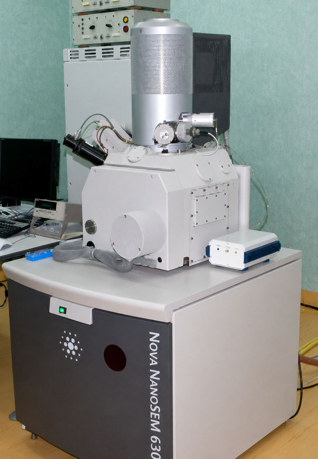

The FEI Nova™ NanoSEM 630 at IMT Bucharest is an advanced ultra-high-resolution field emission scanning electron microscope designed for nanoscale research, sample characterization, analysis, prototyping, and S/TEM sample preparation.
The system provides excellent low-voltage resolution and high surface sensitivity imaging, making it suitable for the investigation of nanostructures, thin films, micro- and nano-devices, and advanced materials. Its high-vacuum imaging capabilities enable ultra-high-resolution characterization down to 1.6 nm at 1 kV, while beam deceleration mode allows sub-100 V imaging with enhanced surface sensitivity.
The instrument also supports low-vacuum and very-low-kV imaging, enabling high-resolution analysis of charging, contaminating, or non-conductive nanomaterials and devices. Backscattered electron imaging can be used for compositional contrast and material characterization in both high- and low-vacuum modes.
The Nova NanoSEM 630 is equipped with a high-stability Schottky field emission gun, providing beam currents up to 100 nA for analytical applications. It also includes a high-precision 150 × 150 mm piezo stage, supporting stable and accurate sample positioning.
In addition to imaging and analysis, the system offers extensive nanoprototyping capabilities, including an onboard 4k × 4k digital pattern generator, dedicated patterning software, a fast electrostatic beam blanker, and gas injection systems for direct electron-beam writing of nanostructures.
Key capabilities include:
- Ultra-high-resolution FE-SEM imaging at high and low voltage
- Resolution of 1.6 nm at 1 kV in high vacuum
- True high-resolution low-vacuum FE-SEM imaging with 1.8 nm resolution at 3 kV
- Beam deceleration mode for sub-100 V, high surface sensitivity imaging
- Low-kV and very-low-kV backscattered electron imaging for compositional characterization
- Imaging of charging, contaminating, and non-conductive nanomaterials
- High-stability Schottky field emission gun with beam current up to 100 nA
- High-precision 150 × 150 mm piezo stage
- Nanoprototyping using digital pattern generation, beam blanking, and gas chemistries
- Applications in nanotechnology, thin films, micro/nano-devices, materials science, and S/TEM sample preparation
This equipment is listed for external research services, equipment sharing, and scientific collaboration through IMT Bucharest. It is not offered for sale.
| Service type | |
|---|---|
| City | |
| Country | |
| Electron Microscopy and Related technique | |
| Producer |





Reviews
There are no reviews yet.